Video lecture: recent topics in diluted magnetic semiconductors

Hideo Ohno from Tohoku University's center for spintronics integrated systems gave a special presentation titled "recent topics in diluted magnetic semiconductors". In his talk, Hideo gives an introduction to ferromagnetic (III,Mn)As and then discusses manipulation by electric-field and materials systems other than (III,Mn)As.

This presentation was given at Keio University's Semiconductor-Spintronics workshop which took place on January 24.
Read the full story Posted: Jan 27,2013

A new technology aims to improving the reliability of spintronics logic ICs

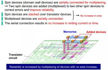
NEC and Tohoku University have developed a new technology that aims to improving the reliability of spintronics logic integrated circuits. This could lead to devices that have a standby power of zero. They have verified this new technology on a prototype chip.

NEC and Tohoku's new device structure connects spin elements in a series, which prevents power consumption from increasing and prevents the area of the circuit from becoming larger. These highly reliable circuit components also support automatic placement and wiring, which means that highly reliable non-volatile logic integrated circuits can be designed even without expertise in spintronics technology.

Read the full story Posted: Jun 18,2012

Tohoku University and Tokyo Electron to jointly develop Spintronics memory technologies

Tohoku University and Tokyo Electron announced that they will jointly develop Spintronics memory integration and manufacturing technology. Professor Tetsuo Endoh from Tohoku's Center for Spintronics Integrated Systems (CSIS) will lead the research. The aim of this project is to present a miniature highly-integrated Spintronics memory device and the process technologies needed to commercially manufacture it.

The CSIS is considered one of the world's leaders in Spintronics memory, and will contribute its magnetic material technologies, device technologies and design technologies. TEL will contribute process and equipment technologies. The video above shows the Spintronics IC work done at the CSIS.

Read the full story Posted: Dec 07,2011

Japanese researchers working on Spintronics based ICs

A group led by Professor Hideo Ohno in the Laboratory of Nanoelectronics and Spintronics, at Tohoku University is working to develop new integrated circuits using spintronics. The ICs store data in nonvolatile memory using magnetism (MRAM), so their standby power can be made zero. This memory utilizes the tunnel magneto-resistance effect.

Read the full story Posted: Mar 24,2010

Researchers prove the existance of a 'Spin battery', might be used to drive cars in the future

Researchers at the University of Miami and at the Universities of Tokyo and Tohoku, Japan, have been able to prove the existence of a "spin battery," a battery that is "charged" by applying a large magnetic field to nano-magnets in a device called a magnetic tunnel junction (MTJ). The new technology is a step towards the creation of computer hard drives with no moving parts, which would be much faster, less expensive and use less energy than current ones. In the future, the new battery could be developed to power cars.

The device created by University of Miami Physicist Stewart E. Barnes, of the College of Arts and Sciences and his collaborators can store energy in magnets rather than through chemical reactions. Like a winding up toy car, the spin battery is "wound up" by applying a large magnetic field --no chemistry involved. The device is potentially better than anything found so far, said Barnes.

Read the full story Posted: Mar 13,2009

Hitachi and RIEC Developed 'Nonvolatile IC' using Spintronics tech based on MTJ device

Hitachi and the Tohoku University's Research Institute of Electrical Communication (RIEC) said they developed a new integrated circuit that integrates an arithmetic function and a nonvolatile memory function by using spintronics and Si technologies.

The IC is made by placing a MTJ (magnetic tunnel junction) MRAM device on a Si chip with a MOS transistor. The data transfer rate is faster, and the IC is small using that method.

The idea is that a circuit that combines memory and a arithmetic unit is faster and smaller 

The prototype chip is a full adder composed of the SUM and CARRY blocks. The SUM block measures 15.5 x 10.7?m, and the CARRY block is 13.9 x 10.7?m. The CMOS logic block was formed with Hitachi's 0.18?m process technology.

Read more here (TechOn japan)

Read the full story Posted: Aug 28,2008