IBM

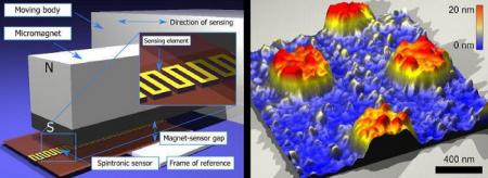
Researchers discover that current flow in a ferromagnetic conductor can produce a magnetic-moment directed spin polarization

Researchers from NYU and IBM Research have created a spintronics device from a ferromagnetic conductor and discovered that current flow in the conductor can produce a spin polarization that is in a direction set by its magnetic moment.

This discovery means that magnetic moment direction can be set in just about any desired direction to then set the spin polarization - this is not possible using the contours of the spin Hall effect in non-magnetic heavy metals.

Read the full story Posted: May 29,2020

IBM developed a Spintronics-based non-contact position sensor

Researchers from IBM Research labs in Zurich developed a Spintronics based small-sized, low cost non-optical, non-contact position sensor. This sensor detect changes in a high-gradient magnetic field of a microscale magnetic dipole. The sensor can achieve sensitivities of up to 40 Ohm/µm, which leads to a noise floor of 0.5 pm/sqrt(Hz) over more than a megahertz bandwidth.

Magnetoresistance-based position sensors have been known for a long time, but their use in nanotechnology was limited due to a relatively low sensitivity and a large amount of hysteresis. These issues were solved by IBM by operating the spintronic sensor close to the pole of a micromagnetic dipole. This is where the magnetic field has an extremely high gradient, which increases as the dimensions of the micromagnet are scaled down.

Read the full story Posted: Jul 23,2014

SRC and DARPA grant $28 million to open a new Spintronics research center

The Semiconductor Research Corporation, and the Defense Advanced Research Projects Agency (DARPA) has awarded a $28 million five-year grant to open the Center for Spintronic Materials, Interfaces, and Novel Architectures, or C-SPIN. This is a multi-university and industry research center that aims to develop technologies for spin-based computing and memory systems. C-SPIN's research areas include perpendicular magnetic materials, spin channel materials (including topological insulators, monolayer MoS2 and graphene), spintronic interface engineering, spin devices and interconnects and spintronic circuits and architectures.

University partners include the University of Minnesota-Twin Cities, Carnegie Mellon University, Cornell University, MIT, Johns Hopkins University and the University of California, Riverside. Industry partners include IBM, Applied materials, Intel, Texas Instruments and Micron.

Read the full story Posted: Jan 18,2013

IBM report advances in spin-based racetrack memory

IBM reports some advances in their racetrack memory program, and they are now able to measure the movement and processing of data as a magnetic pattern on a nanowire (which is 1,000 finer than a human hair).

Racetrack memory uses electron spin to move data on nanowires at hundreds of miles per hour - and has the potential to be very lower power with high densities.

Read the full story Posted: Dec 28,2010

Opening discussion at the International Wafer-Level Packaging Conference about IBM's RaceTrack memory

This year’s fifth annual International Wafer-Level Packaging Conference (IWLPC), October 13-16, 2008 will be the largest ever, according to Dr. Ken Gilleo, IWLPC general chair.

“Exhibitor and attendee interest has been very high, and we anticipate this year’s event will be the largest, as well as the most comprehensive, in our history,” Dr. Gilleo said. With two months to go, the 60-table exhibitor space at our Wyndham Hotel venue is nearly fully occupied.

At a special morning opening address on October 15, 2008, Dr. Stuart Parkin, a Fellow at IBM’s Almaden Research Laboratory, San Jose, California, will discuss “racetrack memory.” Dr. Parkin, a specialist in “spintronics,” will reveal how racetrack memory may lead to solid-state electronics with no moving parts, capable of holding an unparalleled amount of data.

Read the full story Posted: Aug 15,2008

IBM and ETH Zurich university build joint nanotech lab, with Spintronics as one of the research targets

IBM and the ETH Zürich University have agreed to jointly build a laboratory for nanotechnology research. The research activities aim at technologies for the post-CMOS era such as carbon-based materials, nano photonics, spintronics, nanowires and tribology.

The lab will have a 90$ million investment. About one third will go to purchase equipment. The work will begin in Spring 2009, and the activities will start in 2011, and planned to last at least 10 years.

Read the full story Posted: Jun 26,2008

IBM shows New racetrack memory technology

In two papers published in the April 11 issue of Science, IBM Fellow Stuart Parkin and colleagues at the IBM Almaden Research Center in San Jose describe both the fundamentals of a technology dubbed "racetrack" memory as well as a milestone in that technology. This milestone could lead to electronic devices capable of storing far more data in the same amount of space than is possible today, with lightning-fast boot times, far lower cost and unprecedented stability and durability.

Within the next ten years, racetrack memory, so named because the data "races" around the wire "track," could lead to solid state electronic devices - with no moving parts, and therefore more durable - capable of holding far more data in the same amount of space than is possible today. For example, this technology could enable a handheld device such as an mp3 player to store around 500,000 songs or around 3,500 movies - 100 times more than is possible today - with far lower cost and power consumption. The devices would not only store vastly more information in the same space, but also require much less power and generate much less heat, and be practically unbreakable; the result: massive amounts of personal storage that could run on a single battery for weeks at a time and last for decades.

For nearly fifty years, scientists have explored the possibility of storing information in magnetic domain walls, which are the boundaries between magnetic regions or "domains" in magnetic materials. Until now, manipulating domain walls was expensive, complex, and used significant power to generate the fields necessary to do so. In the paper describing their milestone, "Current Controlled Magnetic Domain-Wall Nanowire Shift Register," Dr. Parkin and his team describe how this long-standing obstacle can be overcome by taking advantage of the interaction of spin polarized current with magnetization in the domain walls; this results in a spin transfer torque on the domain wall, causing it to move. The use of spin momentum transfer considerably simplifies the memory device since the current is passed directly across the domain wall without the need for any additional field generators.

Read more here (Nanotechnology now)

Read the full story Posted: Apr 11,2008

IBM teams with TDK to develop STT-RAM

IBM has linked with Japan's TDK to develop so-called spin torque transfer RAM (random access memory) or STT-RAM. In STT-RAM, an electric current is applied to a magnet to change the direction of the magnetic field. The direction of the magnetic field (up-and-down or left-to-right) causes a change in resistance, and the different levels of resistance register as 1s or 0s.

Under the current plan, IBM and TDK, an integral player in magnetic recording components for hard drives, will develop a 65-nanometer prototype within the next four years.

Previously, IBM had been working on a more conventional type of magnetic memory called MRAM. However, the company has been having trouble shrinking the transistors on these chips.

Read the full story Posted: Aug 21,2007